Description
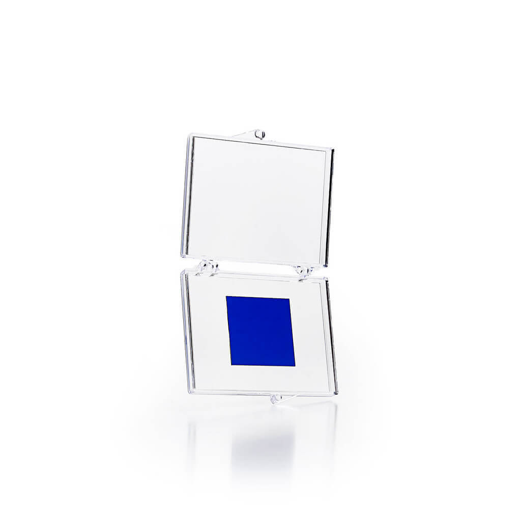
Monolayer Graphene Film on Si-SiO2- 1″ X 1″
Our Monolayer Graphene Film on Si-SiO2- 1″ X 1″ is grown on a 50 micron-thick copper foil that is coated with single atomic layer of graphene which is deposited via chemical vapor deposition (CVD). For products on Si-SiO2 substrates, it is transferred to the substrate using a wet transfer process. Our Monolayer graphene films have the right mix of small size and cost effectiveness to kick start your R&D projects. This product is ideal for R&D departments and universities.
Graphene Film
Transparency: > 97%
Coverage: > 95%
Thickness (theoretical): 0.345 nm
FET Electron Mobility on Al2O3: 2000 cm2/Vs
FET Electron Mobility on SiO2/Si: 4000 cm2/Vs
Sheet Resistance: 580±50 Ohms/sq (1cm x 1cm)
Grain size: Up to 10 μm
Substrate SiO2/Si
Dry Oxide Thickness: 300 nm (+/-5%)
Type/Dopant: P/Bor
Orientation: <100>
Resistivity: <0.005 Ohm·cm
Thickness: 525 +/- 20 μm Front surface:
Single Side Polished Back Surface: Etched
Particles: <10@0.3 μm


